Get Your Free Spectral Analysis Solution.
Tell us about your requirements. Our experts will contact you within 24 hours.
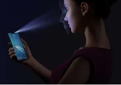
With the development of IoT, AI, and 5G technologies, VCSEL (Vertical Cavity Surface Emitting Laser) technology, as a core technology of 3D imaging and sensing systems, is increasingly gaining attention in applications such as facial recognition, 3D sensing, autonomous driving, gesture detection, and VR (Virtual Reality)/AR (Augmented Reality)/MR (Mixed Reality).
LiSen Optics can provide customers with VCSEL-3D SENSING/TOF detection solutions, including LIV spectrum/power integration testing, NF near-field characteristic testing, FF far-field characteristic testing, BRDF/BTDF optical material AR/VR characteristic testing, and VCSEL-specific integrating spheres. These solutions enable the measurement of energy distribution and uniformity, spectral wavelength and power, near-field and far-field measurements for VCSEL/Mini LED/Micro LED devices, modules, and wafer chips to meet various customized application needs.
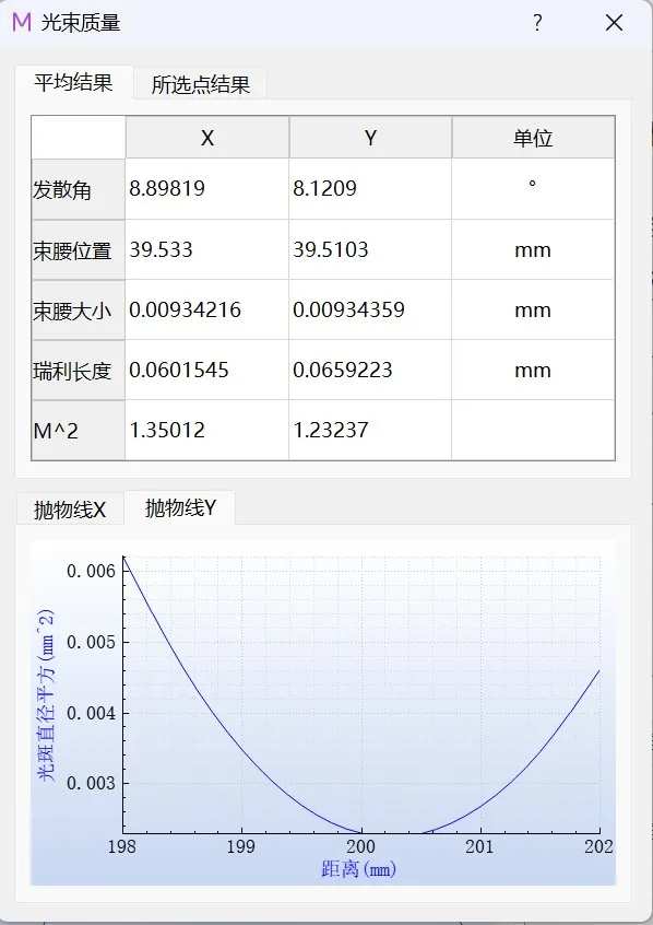
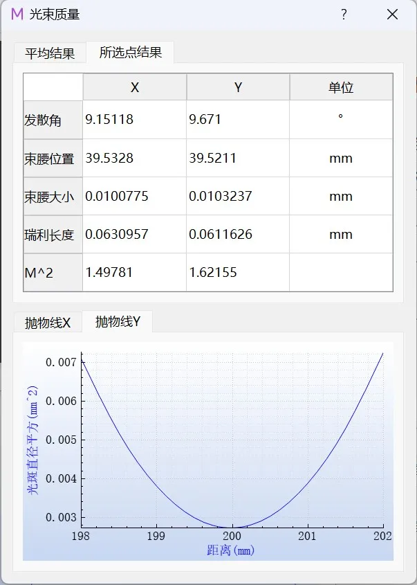
The LS-VCS-NF near-field testing system, developed by LiSen Optics specifically for VCSEL near-field testing, achieves testing of the emission effects, energy distribution, spot size, and stability of VCSEL chips in specific microscopic areas. It can measure the statistics of emission points, mark defective/abnormal points, analyze the consistency of optical power across emission points, beam waist diameter, near-field divergence angle, and beam quality factor M2.
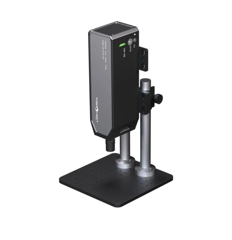
The LS-VCS-NF near-field testing system, developed by LiSen Optics specifically for VCSEL near-field testing, achieves testing of the emission effects, energy distribution, spot size, and stability of VCSEL chips in specific microscopic areas. It can measure the statistics of emission points, mark defective/abnormal points, analyze the consistency of optical power across emission points, beam waist diameter, near-field divergence angle, and beam quality factor M2.
Main Technical Features
● Spectral Range: 400-1000nm / 900-1700nm
● High Data Resolution: Utilizes a 91.7-megapixel camera for data acquisition, ensuring high-resolution data collection.
● Configurable Optical Path: The optical path can rotate the filter wheel based on light intensity and power, selecting attenuators: OD0.3-OD4, with a total of 6 filters.
● Interchangeable Objectives: Different magnification objectives can be replaced as needed, providing more accurate measurements.
● Micro-Beam Waist Laser Measurement: Capable of measuring lasers with a micro-beam waist: ≥10μm with a 10x objective, ≥5μm with a 20x objective.
● Integrated Near-Field Optical Path System: Combines directly coupled imaging lenses and optical path modules in an integrated design.
● Real-Time Monitoring: Real-time statistics of emission points, marking defective/abnormal points, consistency analysis of optical power across emission points, beam waist diameter, near-field divergence angle, and beam quality factor M2.2
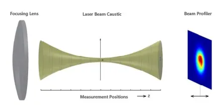
Technical Principle
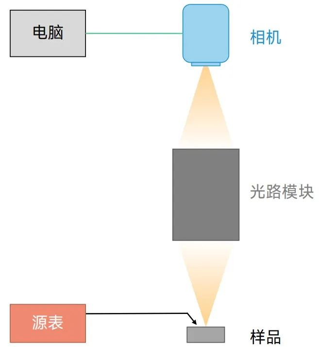
The Principle of Near-Field Testing Module
Technical Principle
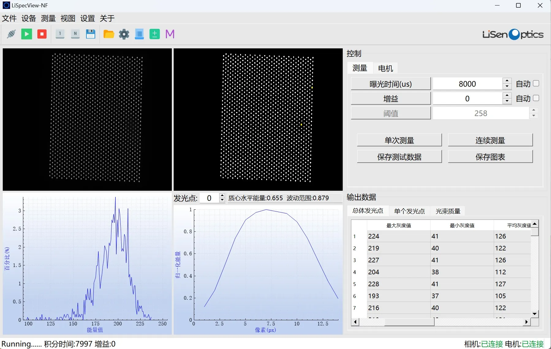
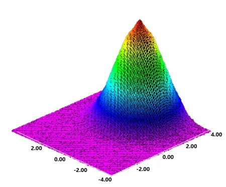
Bad pixel/abnormal pixel mark
 |
 |
|
Average data of all points and its fitted curve |
Selected point (single point) data and its fitting curve |
Technical Principle
 |
 |
|
Vcsel/Micro/Mini LED |
3D Sensing |
 |
 |
|
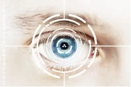
Eye’s Safety |
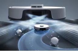
Sweeping Robot |
Technical Principle
The Principle of Near-Field Testing Module
Technical Principle
Bad pixel/abnormal pixel mark
|
|
|
Average data of all points and its fitted curve |
Selected point (single point) data and its fitting curve |
Technical Principle
|
|
|
Vcsel/Micro/Mini LED |
3D Sensing |
|
|
|
Eye’s Safety |
Sweeping Robot |
Technical Indicators
|
Model |
LS-VCS-FF |
|
Spectral Range |
400-1000nm / 900-1700nm |
|
Pixel Resolution |
2592×1944 / 1280×1024 |
|
Target Size |
1/2.8" (5.184mm x 3.888mm) / 1/2" (6.4mm x 5.12mm) |
|
Pixel Size |
2.0 μm / 5.0 μm |
|
Perpendicularity |
<1° |
|
Positioning Accuracy |
0.01mm |
|
Software Testing Functions |
Beam far-field divergence angle, DIP (spot center defect) |
|
Module and Platform |
Far-field optical path module and sample fixture platform |
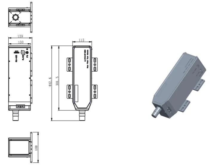
LS-VCS-NF Dimension Drawing(Unit: mm)
Technical Indicators
|
Model |
LS-VCS-FF |
|
Spectral Range |
400-1000nm / 900-1700nm |
|
Pixel Resolution |
2592×1944 / 1280×1024 |
|
Target Size |
1/2.8" (5.184mm x 3.888mm) / 1/2" (6.4mm x 5.12mm) |
|
Pixel Size |
2.0 μm / 5.0 μm |
|
Perpendicularity |
<1° |
|
Positioning Accuracy |
0.01mm |
|
Software Testing Functions |
Beam far-field divergence angle, DIP (spot center defect) |
|
Module and Platform |
Far-field optical path module and sample fixture platform |
LS-VCS-NF Dimension Drawing(Unit: mm)
Get Your Free Spectral Analysis Solution.
Tell us about your requirements. Our experts will contact you within 24 hours.
Focus on spectral sensing and optoelectronic application systems